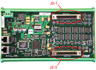
Motor I/O:
SCSI2 Connectors
|
Connector
|
Function
|
|
|
Axes 0 & 1
|
|
|
Axes 2 & 3
|
J0-1 SCSI2 Connector
The wiring of motor I/O on an RMB-10V2-SynqNet is the same as
an Analog-XMP controller once the SynqNet controller has been connected
to the RMB-10V2-SynqNet. For suggested wiring schemes, please click on the reference
link or see the Installing an XMP-Analog
Motion System section in the XMP-Analog Hardware documentation.
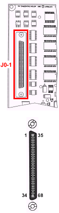 |
Link |
Pin
|
Signal
|
|
Signal
|
Pin
|
Link
|
|
1
|
Analog_IN_0+ |
|
Analog_IN_0- |
35
|
|
|
2
|
Analog_IN_1+ |
|
Analog_IN_1- |
36
|
|
| |
3
|
Gnd |
|
AGnd |
37
|
|
|
4
|
Enc0_A+ |
|
Enc0_A- |
38
|
|
|
5
|
Enc0_B+ |
|
Enc0_B- |
39
|
|
|
6
|
Enc0_I+ |
|
Enc0_I- |
40
|
|
|
7
|
Home0_IN |
|
5V_OUT |
41
|
|
|
8
|
Pos_Lim0_IN |
|
Gnd |
42
|
|
|
9
|
Neg_Lim0_IN |
|
HomeLim0_Rtn |
43
|
|
|
10
|
Cmd_Dac_OUT_0+ |
|
Cmd_Dac_OUT_0- |
44
|
|
|
11
|
Aux_Dac_OUT_0+ |
|
Aux_Dac_OUT_0- |
45
|
|
|
12
|
Amp_Flt0_IN |
|
Amp_Flt0_Rtn |
46
|
|
|
13
|
Amp_En0_Collector |
|
Amp_En0_Emitter |
47
|
|
|
14
|
UserIO_A0 |
|
UserIO_A0_Rtn |
48
|
|
|
15
|
Xcvr0A+ |
|
Xcvr0A- |
49
|
|
|
16
|
Xcvr0B+ |
|
Xcvr0B- |
50
|
|
|
17
|
Xcvr0C+ |
|
Xcvr0C- |
51
|
|
|
18
|
Enc1_A+ |
|
Enc1_A- |
52
|
|
|
19
|
Enc1_B+ |
|
Enc1_B- |
53
|
|
|
20
|
Enc1_I+ |
|
Enc1_I- |
54
|
|
|
21
|
Home1_IN |
|
5V_OUT |
55
|
|
|
22
|
Pos_Lim1_IN |
|
Gnd |
56
|
|
|
23
|
Neg_Lim1_IN |
|
HomeLim1_Rtn |
57
|
|
|
24
|
Cmd_Dac_OUT_1+ |
|
Cmd_Dac_OUT_1- |
58
|
|
|
25
|
Aux_Dac_OUT_1+ |
|
Aux_Dac_OUT_1- |
59
|
|
|
26
|
Amp_Flt1_IN |
|
Amp_Flt1_Rtn |
60
|
|
|
27
|
Amp_En1_Collector |
|
Amp_En1_Emitter |
61
|
|
| |
28
|
Gnd |
|
Gnd |
62
|
|
|
29
|
Xcvr1A+ |
|
Xcvr1A- |
63
|
|
|
30
|
Xcvr1B+ |
|
Xcvr1B- |
64
|
|
|
31
|
Xcvr1C+ |
|
Xcvr1C- |
65
|
|
|
32
|
UserIO_A1 |
|
UserIO_A1_Rtn |
66
|
|
|
33
|
Gp0_04_IN |
|
UserIO_A2 |
67
|
|
|
34
|
NODE_DISABLE |
|
UserIO_A2_Rtn |
68
|
|
|
J2-3 SCSI2 Connector
The wiring of motor I/O on an RMB-10V2-SynqNet is the same as
an Analog-XMP controller once the SynqNet controller has been connected
to the RMB-10V2-SynqNet. For suggested wiring schemes, please click on the reference
link or see the Installing an XMP-Analog
Motion System section in the XMP-Analog Hardware documentation.
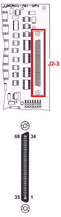 |
Link |
Pin
|
Signal
|
|
Signal
|
Pin
|
Link
|
|
1
|
Enca_A+ |
|
Enca_A- |
35
|
|
|
2
|
Enca_B+ |
|
Enca_B- |
36
|
|
|
3
|
Enca_I+ |
|
Enca_I- |
37
|
|
|
4
|
Enc2_A+ |
|
Enc2_A- |
38
|
|
|
5
|
Enc2_B+ |
|
Enc2_B- |
39
|
|
|
6
|
Enc2_I+ |
|
Enc2_I- |
40
|
|
|
7
|
Home2_IN |
|
5V_OUT |
41
|
|
|
8
|
Pos_Lim2_IN |
|
Gnd |
42
|
|
|
9
|
Neg_Lim2_IN |
|
HomeLim2_Rtn |
43
|
|
|
10
|
Cmd_Dac_OUT_2+ |
|
Cmd_Dac_OUT_2- |
44
|
|
|
11
|
Aux_Dac_OUT_2+ |
|
Aux_Dac_OUT_2- |
45
|
|
|
12
|
Amp_Flt2_IN |
|
Amp_Flt2_Rtn |
46
|
|
|
13
|
Amp_En2_Collector |
|
Amp_En2_Emitter |
47
|
|
|
14
|
UserIO_A3 |
|
UserIO_A3_Rtn |
48
|
|
|
15
|
Xcvr2A+ |
|
Xcvr2A- |
49
|
|
|
16
|
Xcvr2B+ |
|
Xcvr2B- |
50
|
|
|
17
|
Xcvr2C+ |
|
Xcvr2C- |
51
|
|
|
18
|
Enc3_A+ |
|
Enc3_A- |
52
|
|
|
19
|
Enc3_B+ |
|
Enc3_B- |
53
|
|
|
20
|
Enc3_I+ |
|
Enc3_I- |
54
|
|
|
21
|
Home3_IN |
|
5V_OUT |
55
|
|
|
22
|
Pos_Lim3_IN |
|
Gnd |
56
|
|
|
23
|
Neg_Lim3_IN |
|
HomeLim3_Rtn |
57
|
|
|
24
|
Cmd_Dac_OUT_3+ |
|
Cmd_Dac_OUT_3- |
58
|
|
|
25
|
Aux_Dac_OUT_3+ |
|
Aux_Dac_OUT_3- |
59
|
|
|
26
|
Amp_Flt3_IN |
|
Amp_Flt3_Rtn |
60
|
|
|
27
|
Amp_En3_Collector |
|
Amp_En3_Emitter |
61
|
|
| |
28
|
Gnd |
|
Gnd |
62
|
|
|
29
|
Xcvr3A+ |
|
Xcvr3A- |
63
|
|
|
30
|
Xcvr3B+ |
|
Xcvr3B- |
64
|
|
|
31
|
Xcvr3C+ |
|
Xcvr3C- |
65
|
|
|
32
|
Gnd |
|
Gnd |
66
|
|
|
33
|
Analog_IN_2+
|
|
Analog_IN_2-
|
67
|
|
|
34
|
Analog_IN_3+
|
|
Analog_IN_3-
|
68
|
|
|
See Also: General
XMP I/O Specifications
|