RMB-10V2-SynqNet Specifications
Environment | Power | I/O
NOTE 1 : Specifications are across the operating temperature range, except where noted.
See Also: UL Listing and CE Marking
Environment
Parameter |
Specification |
Operating Temp. |
0 - 50 ºC |
Storage Temp. |
0 - 50 ºC |
Humidity |
20 - 90% RH, non-condensing |
Airflow Requirements |
lfm |
Product Certifications |
The RMB-10V2 is not UL/CE certified
See Also
UL Listing and CE Marking |
Power Requirements
Parameter |
Conditions |
Min |
Typ
(25°C) |
Max |
Units |
| Input Voltage |
|
+18 |
+24 |
+30 |
Vdc |
| Input Current |
|
|
0.5 |
1.0 |
Amps |
| Inrush Current |
< 5mS after power-on |
|
4.0 |
5.0 |
Amps |
I/O
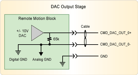
DAC Outputs
Absolute Maximum Ratings |
Parameter |
Rating |
| Output Current |
± 25mA |
Characteristics |
Parameter |
Rating |
| Output Range |
± 10V |
| Output Resolution |
16 bits
0.305 mV per LSB |
| Output Impedance |
0.3 Ω typ. |
| Output Load |
± 5 mA max
2 KΩ min
200 pF max |
| Output at Power-on |
0V
(analog switch to GND) |
| Monotonicity |
16 bit monotonic
No missing codes |
|
Parameter |
Conditions |
Min |
Typ
(25°C) |
Max |
Units |
| Differential Nonlinearity |
|
|
|
± 0.9
± 0.27 |
LSB
mV |
| Integral Nonlinearity |
|
|
± 3
± 0.9 |
± 32
± 10 |
LSB
mV |
| Offset Error |
|
|
± 6
± 2 |
± 21
± 6.5 |
LSB
mV |
| Gain Error |
Load = 10 MΩ
Load = 10 MΩ, at full scale
Load = 10 MΩ, at full scale |
|
± 0.06
± 20
± 6 |
± 0.23
± 75
± 23 |
%
LSB
mV |
| Slew Rate |
|
|
4 |
|
V/µs |
| Settling Time |
to 0.003% FSR |
|
10 |
|
µs |
ADC Inputs
Absolute Maximum Ratings |
Parameter |
Rating |
| Input to AGND |
± 25 V |
Characteristics |
Parameter |
Rating |
| Input Range |
±10V, ±5V, ±2.5V, ±1.25V
software selectable |
| Input Resolution |
16 bits
0.305, 0.152, 0.076, 0.038 mV per LSB |
| Common Mode Voltage |
± 5V max |
| Differential Impedance |
20 MΩ typ |
| Input Filter Bandwidth |
16 kHz @ -3 dB (low pass) |
| Sample Rate |
(see ADC Sample Period) |
|
Parameter |
Conditions |
Min |
Typ
(25°C) |
Max |
Units |
| Differential Nonlinearity |
± 10V range
± 5V range
± 2.5V range
± 1.25V range |
|
|
± 3
± 0.9
± 0.5
± 0.2
± 0.1 |
LSB
mV
mV
mV
mV |
| Integral Nonlinearity |
± 10V range
± 5V range
± 2.5V range
± 1.25V range |
|
|
± 6
± 1.8
± 0.9
± 0.5
± 0.2 |
LSB
mV
mV
mV
mV |
| Offset Error |
± 10V range
± 5V range
± 2.5V range
± 1.25V range |
|
|
± 14
± 9
± 7
± 5 |
mV
mV
mV
mV |
| Gain Error |
Full Scale
± 10V range
± 5V range
± 2.5V range
± 1.25V range |
|
|
± 0.7
± 230
± 70
± 35
± 18
± 9 |
%
LSB
mV
mV
mV
mV |
| Common Mode Rejection @ 1 kHz |
± 10V range
± 5V range
± 2.5V range
± 1.25V range |
|
75
80
84
84 |
. |
dB
dB
dB
dB |
| Crosstalk |
Adjustment
Channels |
|
. |
0.001 |
% |

RS 422 Inputs
Absolute Maximum Ratings |
Parameter |
Rating |
| Input to GND |
-8V to 12.5V |
| ESD Protection |
± 15 kV Human Body Model |
Characteristics |
Parameter |
Rating |
| Differential Termination |
none |
|
Parameter |
Conditions |
Min |
Typ
(25°C) |
Max |
Units |
Input High
Differential Voltage |
|
0.2 |
|
|
V |
Input Low
Differential Voltage |
|
|
|
-0.2 |
V |
Input Common
Mode Voltage |
|
-7 |
|
12 |
V |
| Input Current |
Vin = 12V
Vin = -7V |
-0.8
|
|
1.0
|
mA
mA
|
| Input Impedance |
|
12 |
|
|
kΩ |
| Propagation Delay |
|
|
|
200 |
nS |
RS 422 Outputs
Absolute Maximum Ratings |
Parameter |
Rating |
| ESD protection |
± 15 kV Human Body Model |
| Output Current |
± 50mA |
Characteristics |
Parameter |
Rating |
| Output Protection |
Thermal Shutdown
Current Limiting |
|
Parameter |
Conditions |
Min |
Typ
(25°C) |
Max |
Units |
Output High
Differential Voltage |
50Ω load
no load |
2
|
|
5.5
|
V |
Output Low
Differential Voltage |
50Ω load
no load |
-2
|
|
-5.5
|
V |
Output Common
Mode Voltage |
100Ω load |
|
|
3 |
V |
| Propagation Delay |
|
|
|
60 |
nS |
| Rise Time |
100 pF load |
3 |
20 |
40 |
nS |
| Fall Time |
100 pF load |
3 |
20 |
40 |
nS |
Encoder Inputs
Absolute Maximum Ratings |
Parameter |
Rating |
| Input to GND |
± 25V |
| ESD Protection |
± 15 kV Human Body Model |
Characteristics |
Parameter |
Rating |
| Differential Termination |
100ohm |
| Effective Count Rate |
12.5 MHz max
(digital filter ENABLED)
25 MHz max
(FPGA version x0346 and prior, digital filter DISABLED)
50 MHz max
(FPGA version x0400 and later, digital filter DISABLED) |
| Fault Detection |
(see Broken Wire Fault Detection)
Illegal quadrature transition |
|
Parameter |
Conditions |
Min |
Typ
(25°C) |
Max |
Units |
Input High
Differential Voltage |
Note 2 |
0.2 |
|
6 |
V |
Input Low
Differential Voltage |
Note 2 |
-6 |
|
-0.2 |
V |
Input Common
Mode Voltage |
|
-10 |
|
13.2 |
V |
Input Current
(ignoring 100ohm termination) |
Vin = 13.2V
Vin = -10V |
-0.11
|
|
0.14
|
mA
mA |
Input Impedance
(ignoring 100ohm termination) |
|
90 |
|
|
kΩ |
Fault Detect
Differential Voltage |
|
± 70 |
|
± 250 |
mV |
| Propagation Delay |
|
|
|
75 |
nS |
NOTE 2: An input differential voltage limit of 6V is required to limit power in the 100Ω termination resistor.
Encoder Power Output Pin
Characteristics |
Parameter |
Rating |
| Voltage |
5V ±10% |
| Current |
250 mA max per pin |
| Protection |
Self-healing fuse |
|
Parameter |
Conditions |
Min |
Typ
(25°C) |
Max |
Units |
| Trip Current |
|
|
2.20 |
|
A |
| Hold Current |
|
|
1.10 |
|
A |
| Resistance |
20°C |
0.04 |
|
0.21 |
Ω |
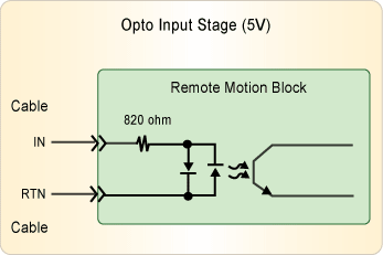
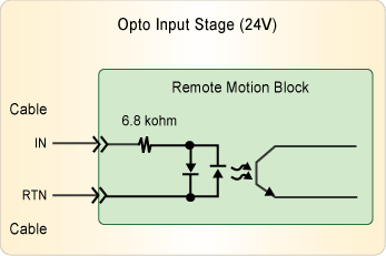
Opto Inputs
Absolute Maximum Ratings |
Parameter |
Rating |
| Isolation to GND |
± 40V |
| Input Voltage |
± 10V max (5V option)
± 30V max (24V option) |
|
Parameter |
Conditions |
Min |
Typ
(25°C) |
Max |
Units |
| Input Active Current |
|
2 |
|
|
mA |
| Input Active Voltage |
5V option
24V option |
3
15
|
|
|
V
V |
| Input Inactive Current |
|
|
|
0.1
|
mA
|
| Propagation Delay |
|
|
|
20 |
µS |
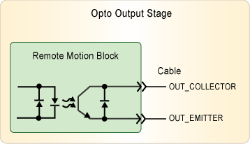
Opto Outputs
Absolute Maximum Ratings |
Parameter |
Rating |
| Isolation to GND |
± 40V |
| Output Current |
50 mA max |
| Output Voltage |
40V max |
| Reverse Voltage |
-0.4V max |
| Reverse Current |
-100mA max |
|
Parameter |
Conditions |
Min |
Typ
(25°C) |
Max |
Units |
| Output Active Current |
|
5 |
|
|
mA |
| Output Active Voltage |
lout = 5mA
lout = 2mA |
|
|
1.1
0.3 |
V
V |
| Output Inactive Leakage Current |
|
|
|
0.01 |
mA |
| Rise Time (see graph) |
10 kΩ load |
|
|
100 |
µS |
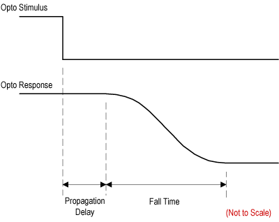
| Fall Time (see graph) |
10 kΩ load |
|
|
100 |
µS |
User I/O Opto Input
Absolute Maximum Ratings |
Parameter |
Rating |
| Isolation to GND |
± 40V |
| Input Current |
50 mA |
|
Parameter |
Conditions |
Min |
Typ
(25°C) |
Max |
Units |
| Input Active Current |
|
2 |
|
|
mA |
| Input Active Voltage |
I = 2mA |
1.9 |
|
|
V |
| Input Inactive Current |
|
|
|
0.1
|
mA
|
| Propagation Delay |
|
|
|
20 |
µS |
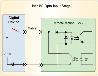
WARNING!
A resistor must be supplied by the digital device. Connecting the RMB's bi-directional opto pins to a power supply will blow the circuit.
Vuser |
R recommended |
5V |
820Ω |
24V |
6.8 kΩ |
User I/O Opto Output
Absolute Maximum Ratings |
Parameter |
Rating |
| Isolation to GND |
± 40V |
| Output Current |
50 mA max |
| Output Voltage |
40V max |
| Reverse Voltage |
-1.5V max |
| Reverse Current |
-50mA max |
|
Parameter |
Conditions |
Min |
Typ
(25°C) |
Max |
Units |
| Output Active Current |
|
5 |
|
. |
mA |
| Output Active Voltage |
lout = 5mA
lout = 2mA |
. |
|
1.1
0.3 |
V
V |
| Output Inactive Leakage Current |
|
|
|
0.01 |
mA |
| Rise Time (see graph) |
10 kΩ load |
|
|
100 |
µS |
| Fall Time (see graph) |
10 kΩ load |
|
|
100 |
µS |
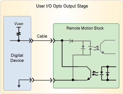
Vuser |
R recommended |
5V |
1.2 kΩ |
24V |
6.8 kΩ |
Opto-isolated Notes
The rise and fall times are the times that the output voltage takes to get from zero to maximum. The rise time is dependent on the load resistor, since that is what's pulling the output up. Other factors include circuit impedance, the stability of the voltage supply, and the quality of the stimulus signal. An ideal circuit will have a response time that is the sum of the specification's propagation delay and rise or fall time. MEI recommends that one assumes that opto-isolated circuits will have a total response time between 100 and 200 microseconds.
Rise Time
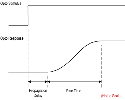
Fall Time
|

