
|
|
| . |
S200: J4
|
||||||||||||||||||||||||||||||||||||||||||||||||||||||||||||||||||||||||||||||||||||||||||||||||||||||||||||||||||||||||||||||||||||||||||||||||
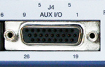 |
See Connector Locations. |
J4 is a 26-Position High Density D subminiature female connector.
|
DINP COM, DINP1, DINP2, DINP3, DINP4
The general purpose inputs are a bank of four inputs that share a common terminal (DINP COM) on J4-1. The inputs operate over a wide input voltage range of ± 4.0 to ± 30 V. General purpose inputs are compatible with either sourcing or sinking currents to provide maximum flexibility for interfacing to field wiring.
Input current is a function of the input voltage and listed in the following table.
Input Voltage (±) |
Input Current (±) |
4.0 V |
0.65 mA |
5.0 V |
0.95 mA |
12 V |
2.5 mA |
24 V |
5.3 mA |
30 V |
6.7 mA |
The response time for DINP1, DINP2, and DINP3 is less than 1 ms. DINP4 has a response time of less than 100 µs.
NOTE: For the fastest response to an input, configure the drive to respond when the input optoisolator is turned ON; current starts flowing in the photo diode.
The list below describes the factory default functions for each of these inputs. A logic input hardware is active when current is flowing through its photo diode. Inactive logic input hardware is open circuited (has no photo diode current). The active control logic polarity of each of these inputs can be set by the corresponding DInpxPol NV Parameter. In other words, depending on the state of DInpxPol, a given hardware input driven active, will activate or not activate a drive control function.
DINP1 (ENABLE) Input 1
The ENABLE control function mapped to this input enables/disables the drive and resets the latched drive faults. With default logic polarity (DInp1Pol = Normal), the drive can enable when input 1 is activated (current flowing in the photo diode) and will be disabled when open circuited. This input will disable a drive independent of any other parameters. Successful enabling requires no drive faults and SWEnable, SynqNet drive enable active as appropriate. Setting this input to the inactive state clears any latched drive faults.
DINP2 (INHIBIT+) Input 2
The INHIBIT+ control function mapped to this input prevents further motion in the clockwise shaft motion direction when activated by current flowing in the photo diode. This input has no effect on motion in the counter-clockwise direction. This function can be turned on or off by setting EnInhibitCW. DInp2Pol sets the control logic active polarity for this hardware input.This input is useful for a clockwise over travel limit switch. Broken wire “failsafe” over travel limit switch operation requires that DInp1Pol be set to Invert by the user to change the factory default.
NOTE: For S200 drives with the SynqNet option, the base drive INHIBIT+ function is turned off by EnInhibitCW = Off. Over travel limit switch inputs must be wired directly to J13 on the SynqNet option card.
DINP3 (INHIBIT-) Input 3
This input operates symmetrically to DINP2 with the INHIBIT- control function preventing further motion in the counter-clockwise shaft motion direction. This function can be turned on or off by setting EnInhibitCCW. DInp3Pol sets the control logic polarity.
DINP4 (DIRECTION) Input 4
This input is the direction input when the drive is in Position Mode with the PosCmdSrc set to Step & Direction. Open circuit/no LED current positively increments the position command/motor goes CW. Set up time for direction is 100 µs. Minimum pulse width is 200 µs. Refer to DInp4.
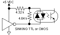
Sinking Logic
For compatibility with sinking outputs, the DINP COM terminal is connected to the positive terminal of a power source (4.0 to 30 VDC). The input (DINP1-4) is connected to the sinking logic output of the field device as shown in the diagram below.
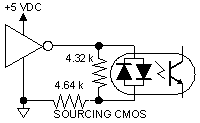
Sourcing Logic
For compatibility with sourcing outputs, the DINP COM terminal is connected to the negative terminal of the power source (4.0 to 30 VDC). The input (DINP1-4) is connected to the sourcing logic output on the field device as shown in the diagram below.
TTL and CMOS Drivers
The following are examples of driving with TTL or CMOS output devices.
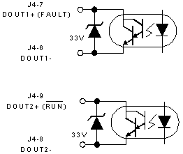
J4-6,7 DOUT1 (FAULT)
J4-8,9 DOUT2 ( RUN )
DOUT1 and DOUT2 are optically isolated outputs that provide information about the state of the drive. The outputs are Darlington phototransistors with a 33 V zener diode wired in parallel to clamp voltage transients.
The following table lists the maximum output rating.
Parameter |
Rating |
Maximum Voltage |
30 VDC |
Maximum Current |
50 mA |
| VON | 1.0 V at 10 mA 1.2 V at 50 mA |
| IOFF | 5 µA |
| Response time | 1 ms |
| Clamp Voltage | 33 V (nominal) |
WARNING: The outputs are not short circuit protected. Configure the application to ensure the maximum current is not exceeded.
The list below describes the factory defaults for each of the outputs.
DOUT1 (FAULT) Output 1
This output provides the FAULT state of the drive. When the drive is powered and not faulted, the output transistor is turned ON. When the drive is faulted or not powered, the output transistor is turned OFF.
DOUT2 (RUN) Output 2
This output provides the RUN state of the drive. When the drive is powered, not faulted and enabled, the output transistor is turned ON. When the drive is faulted, not enabled or not powered, the output transistor is turned OFF. This output indicates when the drive is capable of running the motor.
Both the collector and emitter of the phototransistor are on J4, providing the capability to drive either sinking or sourcing loads.
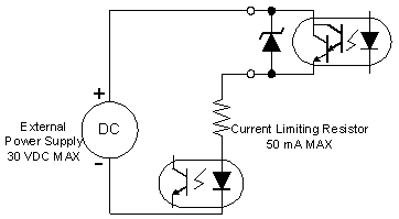
An optoisolator is being driven in this example. The current through the output needs to be limited to 50 mA or less, which is accomplished by selecting an appropriate current limiting resistor. The voltage of the external power source needs to be 30 VDC or less, and can be the same source used to provide power to the inputs.
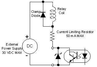
In this example, a relay coil is being driven. The current through the coil needs to be limited to 50 mA or less, which is accomplished by selecting an appropriate value of current limiting resistor.
The voltage of the external power source needs to be 30 VDC or less and can be the same source used to provide power to the inputs. A clamp diode must be added across the coil to clamp the voltage during turn-off.
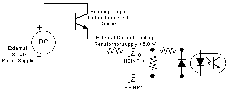
J4-10, 11 HSINP1+, HSINP1- (STEP/PWM)
The S200 has one high speed input for use with PWM input commands or with Step Input in Position Mode.
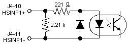
The high speed input works directly with 5 V input, 3.0 to 6.0 V range, without the use of a current limiting resistor. To operate the input with voltages higher than 5 V, an external current limiting resistor is required in series with the input. The input current should be in the range of 9 to 24 mA for proper operation. The following table lists the recommended current limiting resistors for supply voltages greater than 5 V.
Supply Voltage |
Current Limiting Resistor |
5 V |
None |
12 V |
360 Ω, ¼ watt, resistor |
24 V |
1000 Ω, ½ watt, resistor |
In Step-Dir Position Mode the transition edge from LED current to no LED current yields a step count. The transition edge from no LED current to LED current yields no action.
NOTE: Maximum step frequency is 1.5 MHz. Minimum pulse width is 250 ns.
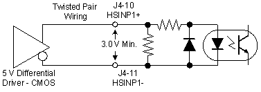
NOTE: For single ended operation, it is recommended that both wires (J4-10 and J4-11) run in the cable be terminated at the control source (differential noise).
High Speed Input Differential Drive
A differential drive is recommended for the Step Input. To provide maximum noise immunity, drive the high speed input differentially from 5 volt logic through twisted pair wiring. The differential driver needs to deliver a minimum of 3.0 V to the input terminals on J4. A CMOS driver is recommended.
For single ended operation, both terminals of the high speed input are available on J4, allowing the input to be connected to either sinking or sourcing logic. The following diagram shows the connections to drive the high speed input from sinking logic.
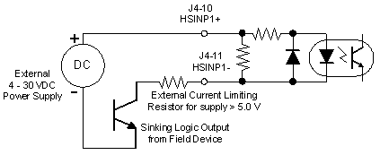
The following shows the connections to drive the high speed input from sourcing logic. The power supply can be the same power source used to provide power for the general purpose inputs.
J4-12 SFD BAT+
The SFD BAT+ terminal is an optional feature and is not required for proper operation of the drive. It is only required if battery backup of the multi-turn information is required from the SFD. If the feedback device is not an SFD, then the battery does nothing.
J4-13 I/O RTN
The I/O RTN is the ground reference for the SFD BAT+ input.
J4-14 DAC MON1
J4-15 DAC MON2
The DAC Monitors are general-purpose analog monitor points. The output range is 0.5 to 4.5 V with a source impedance of 2.9 kW, which limits the short circuit to I/O RTN to 2 mA. Each DAC Monitor can be mapped by software to one of a number of internal variables.
J4-13, 16, 23, 26 I/O RTN
I/O RTN is the ground reference for the DAC MON, Analog Command, Encoder output/inputs, and SFD BAT+. These pins are electrically shorted together inside the drive.
NOTE: Connect one of the I/O RTN pins to an earth ground point in the cabinet reserved for single point grounding of all returns (drives and supplies) to control common mode voltage.
J4-19 CH A OUT/IN
J4-20 CH A OUT/IN
J4-21 CH B OUT/IN
J4-22 CH B OUT/INOutputs
Channels A and B are RS-485 compliant differential I/O that can be configured as either inputs or outputs. Default is as outputs. When configured as outputs and with high resolution feedback such as the SFD device, Channels A and B provide position signals generated from the feedback device that emulate a quadrature encoder.
The outputs are buffered by 5.0 V, 75LBC170 type RS-422 compatible line drivers. Recommended load current is ±20 mA, which corresponds to a line-to-line load resistance of 100 Ω. These outputs can handle shorts to I/O RTN indefinitely without damage.
The resolution of the Encoder Outputs (number of pulses per motor revolution), is set by S1 (rotary switch), as follows:
S1 Position |
Encoder Pulses/Revolutions |
0 |
User settable1 (factory default = 500) |
1 |
512 |
2 |
1000 |
3 |
1024 |
4 |
2000 |
5 |
2048 |
6 |
4096 |
7 |
5000 |
8 |
8192 |
9 |
10000 |
| 1 - User settable non-volatile PPR via the serial port. Possible PPR are:128, 512, 1024, 2048, 4096, 8192, 16384, 32768, 125, 500, 1000, 2000, 2500, 5000, 10000, 20000 | |
The maximum output line frequency is 2.5 MHz. Limit line frequency to below 1.25 MHz, which corresponds to quadrature count frequency below 5 MHz, for robust operation.
NOTE: The emulated encoder output is only available when using a high resolution feedback device such as the SFD Feedback to the base unit or Encoder feedback to the option card. The emulated encoder outputs have no signals when there is only base unit 6-step feedback.
Inputs
Channels A and B can be configured as inputs by setting NV Parameter PosCmdSrc to AQUADB. With NV Parameter OpMode set to Position and PosCmdSrc to AQUADB, the motor shaft position command comes from the quadrature decode of channels A and B input scaled by the ratio of NV Parameters GearOut over GearIn.
(See the Control Mode tab in S200Tools.)
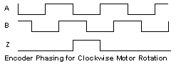
In Input mode, Channels A & B accept quadrature position commands. The command signals need to be differential quadrature signals.
Channel A leading B generates a CW command position while Channel B leading A generates a CCW position command. The magnitude of the position command is set by GearIn and GearOut. The maximum input line frequency for reliable operation is 625 kHz, which corresponds to a maximum quadrature pulse rate of 2.5 MHz.
J4-17, 18 CH Z OUT CH Z OUT
The CH Z Output is only available when using SFD Feedback. These two terminals function as a differential, TTL marker pulse. The output pulse occurs once per motor shaft revolution, starting at feedback device position = 0. Its width is one line width or two quadrature encoder widths. The CH Z uses the same differential driver as described for CH A and CH B.
Encoder Phasing
ANA CMD J4-24, 25(+), (-) Inputs
This differential input accepts the analog command from the user. It has a maximum single ended input range with respect to I/O RTN on either input of –12.5 to +15.5 VDC, a differential input impedance of > 300 kΩ, and a single ended impedance of > 150 kΩ. The recommended full-scale differential command input range is ±10 V, but the input can handle up to ±12 V to accommodate noise and overshoot spikes. Default setup has ±10 V corresponding to ±Ipeak or ± maximum velocity depending on the OpMode.
The offset, gain (including polarity), and low pass filter bandwidth of this input are set by the following NV Parameters: CmdGain, CmdOffset, and CmdF0 respectively and can be adjusted by the PC setup software. Defaults are ±10 V range, 0 offset, 1500 Hz bandwidth. Positive ANA CMD yields clockwise torque when looking at the shaft at the front of the motor.
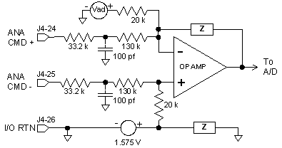
NOTE: Always connect I/O RTN (J4-26) to the signal ground of the source. Failure to do so may result in erratic operation.
Both J4-24 and J4-25 need to be wired. For single ended operation, connect the unused input to the signal ground of the source. For optimal signal fidelity, use a separate wire all the way back to the source for the unused input connection to the source’s signal ground.
The direction of rotation of the motor can be changed by swapping the ANA CMD input connections or changing the sign of the CmdGain NV Parameter.
26-Pin Male High Density D-Sub with Back shell Kit
24 AWG Max., NorComp 180-026-102-001 – D-Sub Connector
NorComp 978-015-010-03-1 – Back shell kit
Refer to www.norcomp.net
| | | Copyright © 2001-2021 Motion Engineering |
