TSIO-9001; 5Vdc Counter
Counter; High Speed; 1 Channel; 5V
|
|
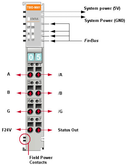
- The module is 1 Channel Vdc type incremental encoder interface.
It has 1 channel output for status.
- The module is capable of counting binary pulses and transmits
the data to the field bus.
- The module has 5 status LEDs.
(1- network status, 5- field device status)
|
| Input Specification
|
| Number of Inputs |
0-1 group of A and / A (or GND)
2-3 group of B and / B (or GND)
4-5 group of G and / G (or GND) |
| LED Indicators |
5 green for Input status
|
| Input Voltage |
5Vdc |
| Input Current |
16.2mA @ 5Vdc |
| Input ON-state Current |
Input Current > 5mA |
| Input ON-state Voltage |
Input Voltage > 2.6Vdc |
| Output ON-state Current |
Output Current < 0.25mA
|
| Output ON-state Voltage |
Output Voltage < 1.25Vdc |
| Max. ON-state Voltage |
6V |
| Max. Input Frequency |
Max. 1.5 MHz |
| Input Filter Selections |
Bypass
1usec
5usec
10usec
50usec
100usec
500usec
1msec
5msec
10msec |
| Output Specification
|
| Number
of Outputs |
6-7 Status or Digital Output |
| LED Indicators |
1 green for Output status
|
| Output Control |
Programmable Outputs. See Output
Data. |
| Output Supply Voltage
Range |
5 to 28.8Vdc (HSC Status output) |
| ON-state Voltage Drop |
Max. 0.3Vdc |
| ON-state Current |
Max. 1mA |
| OFF-state Leakage |
Max. 0.5mA |
| Output Signal Delay |
OFF to ON: Max. 0.5ms
ON to OFF: Max. 1ms |
| Output Current Rating |
Max. 0.5A |
| Surge Current |
1.5A for 10ms, repeatable every 3
sec |
| Fusing |
Outputs are electronically protected |
| Output Type |
Sinking type |
| Over current protection |
1.8A (Shutdown Current) |
| General Specification |
| ID |
0x340501C1 |
| Logic Power Dissipation |
80mA Max. @ 5.0Vdc |
| Isolation |
I/O to Logic: Photocoupler
isolation |
Operating Temperature
Non-Operating Temperature
Relative Humidity
Operating Altitude
Shock Operating
Shock Non-Operating
Vibration
Mounting |
–20 to 55°C (–4 to 131°F)
–20 to 55°C (–4 to 131°F)
5 to 95% non-condensing
2000m
30g
50g
2g @ 10 to 500Hz
DIN rail or screw
|
| I/O Cables |
Max. AWG 14 |
| Weight |
70g |
| Module Size |
67mm x 12mm x 95mm
(H x W x L) |
| Environmental Requirements |
See Environment
Requirements |
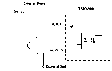
Open Collector Sensor Interface Example
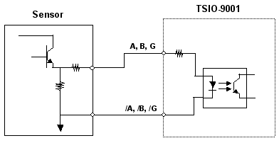
Voltage Output Sensor Interface Example
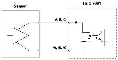
Line Drive Sensor Interface Example
Status Output (Sink)
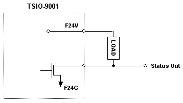
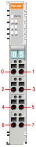
Pinouts
 |
|
Pin No.
|
Description
|
|
0
|
A Pulse Input |
|
1
|
/A Pulse Input or Gnd |
|
2
|
B Pulse Input |
|
3
|
/B Pulse Input or Gnd |
|
4
|
G Pulse Input |
|
5
|
/G Pulse Input or Gnd |
|
6
|
F24V |
|
7
|
Status Output (Sink) |
|
Parameters
Parameter 0 and Parameter 1 can be set to change the counter modes, input filter, and gate settings. TSIO-9001 has seven major counting modes.
| |
- 1 Pulse Mode (A:Pulse, B:Direction)
- 2 Pulse Mode (A:Pulse, B:Direction)
- Encoder x1 (A:Aph, B:Bph)
- Encoder x2 (A:Aph, B:Bph)
- Encoder x4 (A:Aph, B:Bph)
- Period/Rate Mode
- PWM Output Mode (Gate Function Disabled)
|
Parameter |
Access |
Decimal
Bit |
Description |
0
|
Read
and
Write
|
0-3 |
3 |
2 |
1 |
0 |
Counter Mode |
0 |
0 |
0 |
0 |
Counter Disabled |
0 |
0 |
0 |
1 |
1 Pulse Mode
(A:Pulse, B:Direction) |
0 |
0 |
1 |
0 |
2 Pulse Mode
(A:Up Pulse, B:Down Pulse) |
0 |
0 |
1 |
1 |
Encoder x1
(A:Aph, B:Bph) |
0 |
1 |
0 |
0 |
Encoder x2
(A:Aph, B:Bph) |
0 |
1 |
0 |
1 |
Encoder x4
(A:Aph, B:Bph) |
0 |
1 |
1 |
0 |
Period/Rate Mode
(Gate Function Disabled) |
0 |
1 |
1 |
1 |
Reserved |
1 |
0 |
0 |
0 |
PWM Output Mode
(Gate Function Disabled) |
1 |
0 |
0 |
1 |
Reserved |
Others |
Counter Disabled |
4-7 |
7 |
6 |
5 |
4 |
Gate Function |
0 |
0 |
0 |
0 |
Gate Function Disabled |
0 |
0 |
0 |
1 |
Store/Continue |
0 |
0 |
1 |
0 |
Store/Wait/Resume |
0 |
0 |
1 |
1 |
Store-Reset/Wait/Start |
0 |
1 |
0 |
0 |
Store-Reset/Start |
|
Others |
Gate Function Disabled |
1 |
Read
and
Write |
0-3 |
3 |
2 |
1 |
0 |
Input Filter |
| 0 |
0 |
0 |
0 |
Bypass(about 1.5Mhz) |
| 0 |
0 |
0 |
1 |
1usec(500Khz ± 35%) |
| 0 |
0 |
1 |
0 |
5usec(100Khz ± 35%) |
| 0 |
0 |
1 |
1 |
10usec(50Khz ± 35%) |
| 0 |
1 |
0 |
0 |
50usec(10Khz ± 35%) |
| 0 |
1 |
0 |
1 |
100usec(5Khz ± 35%) |
| 0 |
1 |
1 |
0 |
500usec(5Khz ± 35%) |
| 0 |
1 |
1 |
1 |
1msec(500hz ± 35%) |
| 1 |
0 |
0 |
0 |
5msec(100hz ± 35%) |
1 |
0 |
0 |
1 |
10msec(50hz ± 35%) |
Others |
Bypass(about 1.5Mhz) |
4-7 |
7 |
6 |
5 |
4 |
Gate Sampling Time |
| 0 |
0 |
0 |
0 |
(10/1) Mhz (0.1us) |
| 0 |
0 |
0 |
1 |
(10/2) Mhz (0.2us) |
| 0 |
0 |
1 |
0 |
(10/4) Mhz (0.4us) |
| 0 |
0 |
1 |
1 |
(10/8) Mhz (0.8us) |
| 0 |
1 |
0 |
0 |
(10/16) Mhz (1.6us) |
| 0 |
1 |
0 |
1 |
(10/32) Mhz (3.2us) |
| 0 |
1 |
1 |
0 |
(10/64) Mhz (6.4us) |
| 0 |
1 |
1 |
1 |
(10/128) Mhz (12.8us) |
|
Others |
(10/1) Mhz (0.1us) |
Counter Mode
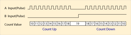
1 Pulse Mode (A:Pulse, B:Direction)
The 1 Pulse Mode reads incoming pulses and returns a binary number (0 to 16,777,215) to the FnBus. The 1 Pulse Mode accepts only one-phase input. Setting pulse B determines the counter direction.
B "High" : Down Counter
B "Low" : Up Counter
| Bit |
7 |
6 |
5 |
4 |
3 |
2 |
1 |
0 |
| Counter Mode |
|
|
|
|
0 |
0 |
0 |
1 |
The diagram below shows the timing waveforms of 1 Pulse Method Pulse Mode.
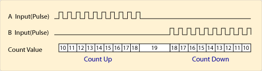
2 Pulse Mode (A:Up Pulse, B:Down Pulse)
The 2 Pulse Mode reads incoming pulses and returns a binary (0 to 16,777,215) to FnBus. The 2 Pulse Mode only accepts 2 Phase input.
A "Low" : Counts down on rising edge input pulse B.
B "Low : Counts up on rising edge input pulse A.
| Bit |
7 |
6 |
5 |
4 |
3 |
2 |
1 |
0 |
| Counter Mode |
|
|
|
|
0 |
0 |
1 |
0 |
The diagram below shows the timing waveforms of 2 Pulse Mode.
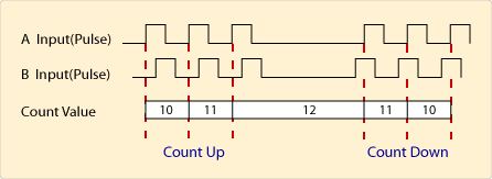
Encoder x1 (A:Aph, B:Bph)
The Encoder x1 reads incoming pulses and returns a number (0 to 16,777,215) to the FnBus. The Encoder x1 only accepts 2 Phase quadrature (90º) inputs. The mode senses the relationship between the 2 Phase, and counts up or down accordingly.
| Bit |
7 |
6 |
5 |
4 |
3 |
2 |
1 |
0 |
| Counter Mode |
|
|
|
|
0 |
0 |
1 |
1 |
The diagram below shows the timing waveforms of Encoder Mode x1.
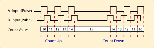
Encoder x2 (A:Aph, B:Bph)
The Encoder x2 reads incoming pulse and returns a number (0 to 16,777,215) to the FnBus. The Encoder x2 only accepts 2 Phase quadrature (90º) inputs. The mode senses the relationship between the 2 Phase, and counts up or down accordingly.
| Bit |
7 |
6 |
5 |
4 |
3 |
2 |
1 |
0 |
| Counter Mode |
|
|
|
|
0 |
1 |
0 |
0 |
The diagram below shows the timing waveforms of Encoder Mode x2.
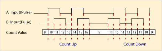
Encoder x4 (A:Aph, B:Bph)
The Encoder x4 reads incoming pulse and returns number (0 to 16,777,215) to the FnBus. The Encoder x4 only accepts 2 Phase quadrature (90º) inputs. The mode senses the relationship between the 2 Phase, and counts up or down accordingly.
| Bit |
7 |
6 |
5 |
4 |
3 |
2 |
1 |
0 |
| Counter Mode |
|
|
|
|
0 |
1 |
0 |
1 |
The diagram below shows the timing waveforms of Encoder Mode x4.
Period/Rate Mode (Gate Function Disabled)
The Period/Rate Mode will return the total Current Count Value to the FnBus, by gating an Internal Sampling Clock with an external signal.
Using the total number of input pulses and the internal sampling clock rate we can calculate the incoming frequency of the G Input (Pulse).
The count value is calculated by the following equation:
Stored Count Value = (1/2fin) / GT where, GT=Gate Time, fin = Input Frequency
Using the same equation, we can also determine the frequency.
Frequency = 1 / (2 * GT * Count)
where, GT = Gate Time = 1 / fclock = 1 / 10MHz = 0.1S and, fclock = Clock Frequency
| Bit |
7 |
6 |
5 |
4 |
3 |
2 |
1 |
0 |
| Counter Mode |
|
|
|
|
0 |
1 |
1 |
0 |
The diagram below shows the timing waveforms of Period/Rate Mode.
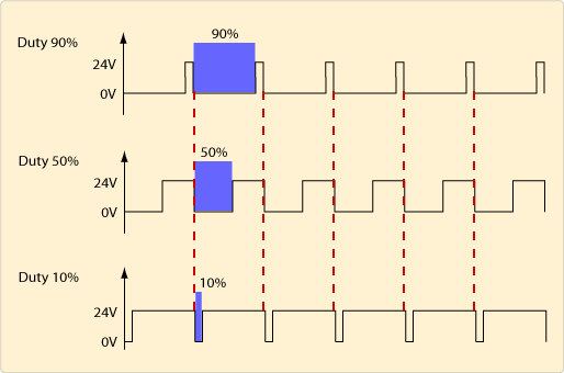
PWM (Pulse Width Modulation) Output Mode
The PWM Output Mode uses the Current Counter Value to generate a continuous rolling sequence of numbers. The configurations of the PWM has a frequencey range of (1 to 20Khz) and a duty cycle of (0 to 100%). The PWM output can be used to direct the PWM signal to terminal output.
| Bit |
7 |
6 |
5 |
4 |
3 |
2 |
1 |
0 |
| Counter Mode |
|
|
|
|
1 |
0 |
0 |
0 |
The diagram below shows the timing waveforms of PWM Output Mode.
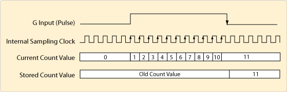
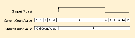
Gate Function Mode
Store/Continue
On a G input rising edge, the Stored Count Value register will get the counting value from the Current Count Value register. The Current Count Value will continue to count.
| Bit |
7 |
6 |
5 |
4 |
3 |
2 |
1 |
0 |
| Gate Function |
0 |
0 |
0 |
1 |
|
|
|
|
The diagram below shows the timing waveforms of Store/Continue.

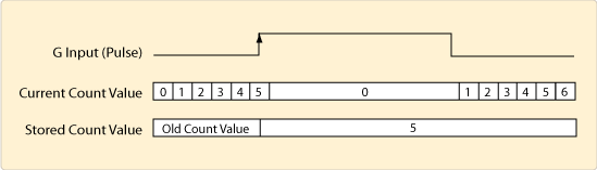
Store/Wait/Resume
On a G input rising edge, the Stored Count Value register will get the counting value from the Current Count Value register and waits for the Current Count Value until the falling edge. Counting will resume on the falling edge.
| Bit |
7 |
6 |
5 |
4 |
3 |
2 |
1 |
0 |
| Gate Function |
0 |
0 |
1 |
0 |
|
|
|
|
The diagram below shows the timing waveforms of Store/Wait/Resume.
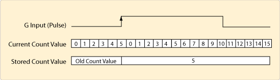
Store-Reset/Wait/Start
On a G input rising edge, the Stored Count Value register will get the counting value from the Current Count Value register and then resets the Current Count Value register. Counting will resume on the falling edge.
| Bit |
7 |
6 |
5 |
4 |
3 |
2 |
1 |
0 |
| Gate Function |
0 |
0 |
1 |
1 |
|
|
|
|
The diagram below shows the timing waveforms of Store-Reset/Wait/Start.
Store-Reset/Start
On a G input rising edge, the Stored Count Value register will get the counting value from the Current Count Value register and then resets the Current Count Value register. Counting will resume immediately after the reset.
| Bit |
7 |
6 |
5 |
4 |
3 |
2 |
1 |
0 |
| Gate Function |
0 |
1 |
0 |
0 |
|
|
|
|
The diagram below shows the timing waveforms of Store-Reset/Wait/Start.
Memory
Memory |
Access |
Description |
Default |
0
|
Read
|
Current Count Value (Low byte) (Input Data Byte 0) |
0 |
1
|
Read
|
Current Count Value (Middle byte) (Input Data Byte 1) |
0 |
2
|
Read
|
Current Count Value (High byte) (Input Data Byte 2) |
0 |
3
|
Read
|
Always 0 (Input Data Byte 3) |
0 |
4
|
Read
|
Status Low (compared flags) (Input Data Byte 4) |
0 |
5
|
Read
|
Status High (same as LED display) (Input Data Byte 5) |
0 |
6
|
Read
|
Output Terminal (OT) Control (Output Data Byte 0) |
0 |
7
|
Read
|
SSR (Special Selection Register)(Output Data Byte 1) |
0 |
8
|
Read
and
Write
|
Gate Function/Counter Mode (Parameter Byte 0) |
0 |
9
|
Read
and
Write
|
Gate Sampling Time/Input Filter (Parameter Byte 1) |
0 |
10
|
Read
and
Write
|
Not Used |
0 |
11
|
Read
and
Write
|
Not Used |
0 |
12
|
Read
|
Stored Count Value (Low byte) (Input Data Byte 0) |
0 |
13
|
Read
|
Stored Count Value (Middle byte) (Input Data Byte 1) |
0 |
14
|
Read
|
Stored Count Value (High byte) (Input Data Byte 2) |
0 |
15
|
Read
|
Always 0 (Input Data Byte 3) |
0 |
16
|
Read
and
Write
|
Initial Counter Value (Low byte)
(Initial counter or PWM Frequency value)
|
0 |
17
|
Read
and
Write
|
Initial Counter Value (Middle byte)
(Initial counter or PWM Frequency value)
|
0 |
18
|
Read
and
Write
|
Initial Count Value (High byte)
(Initial counter or PWM Frequency value)
|
0 |
19
|
Read
and
Write
|
Always 0 |
0 |
20
|
Read
and
Write
|
Compare Count Value (Low byte) |
0 |
21
|
Read
and
Write
|
Compare Count Value (Middle byte) |
0 |
22
|
Read
and
Write
|
Compare Count Value (High byte) |
0 |
23
|
Read
and
Write
|
Always 0 |
0 |
I/O Data
Input Data
| |
|
|
Bit No.
|
Decimal Bit
|
|
Bit7
|
Bit6
|
Bit5
|
Bit4
|
Bit3
|
Bit2
|
Bit1
|
Bit0
|
|
Byte 0
|
Current Count Value (Low) when IDS
= 0
Stored Count Value (Low) when IDS = 1
|
|
Byte 1
|
Current Count Value (Middle) when
IDS = 0
Stored Count Value (Middle) when IDS = 1
|
|
Byte 2
|
Current Count Value (High) when IDS
= 0
Stored Count Value (High) when IDS = 1
|
|
Byte 3
|
Always 0
|
|
Byte 4
|
Status Low (compared flags)
|
|
0
|
0
|
SUF
|
SOF
|
SEQ(=)
|
SEQ(=)
|
SLT(<)
|
SGT(>)
|
|
Byte 5
|
Status High (same as LED display)
|
|
0
|
0
|
SOT
|
SGIN
|
SBIN
|
SAIN
|
SDN
|
SUP
|
|
Byte 4
SUF - Status Underflow (Latched)
SOF - Status Overflow (Latched)
SEQ(=) - Status Current Count Value = Compare Count Value
(Unlatched)
SLT(<) - Status Current Count Value < Compare Count
Value (Unlatched)
SGT(>) - Status Current Count Value > Compare Count
Value (Unlatched)
Byte 5
SOT - Status Output Terminal
SGIN - Status G Terminal Input
SBIN - Status B Terminal Input
SAIN - Status A Terminal Input
SDN - Status Counter Down
SUP - Status Counter Up
|
|
Output Data
| |
|
Bit No. |
Decimal Bit |
Bit7 |
Bit6 |
Bit5 |
Bit4 |
Bit3 |
Bit2 |
Bit1 |
Bit0 |
Byte 0 |
Output Terminal Control |
Output Terminal Selection
"0000": Force OFF
"0001": Greater Than
"0010": Less Than
"0011": Equal To
"0101": Overflow
"0110": Underflow
"1001": Count Up
"1010": Count Down
"1011": A Terminal Input
"1100": B Terminal Input
"1101": G Terminal Input
"1110": PWM Output
"1111": Force ON
others: Force OFF |
Output Terminal Pulse Width
"0000": Bypass
"0001": 1msec
"0010": 5msec
"0011": 10msec
"0100": 20msec
"0101": 50msec
"0110": 100msec
"0111": 200msec
"1000": 500msec
"1111": Latched
others: Bypass |
Byte 1 |
Command or PWM duty value (PWM Output Mode) |
| Command |
7bit |
6bit |
5bit |
4bit |
3bit |
2bit |
1bit |
0bit |
HRST |
CR |
CP |
CST |
PU |
PO |
PE |
IDS |
| PWM Duty Value |
0 to 100dec (= 0 to 100%) |
|
Byte 1
HRST - HSC Reset
CR - Counter Reset, Current Count Value = 0
CP - Counter Reset, Current Count Value = Initial Count Value
CST - Clear Status (SOT, SUF, SOF, SEQL)
PO - Process Overflow
PE - Process Equal
IDS - Input Data Selection (0 : Current Count Value, 1 : Store
Count Value)
|
|
Slice Status LED
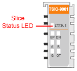
State |
LED |
Description |
Not Powered,
Not Initialized |
OFF |
The slice is either not powered or has not been initialized. |
| Normal Communication |
Green
|
Slice to network adapter communication is operating normally. |
| Communication Ready |
Flashing Green |
Slice to network adapter communication is ready to be started. |
| Communication Fault |
Flashing Red |
Slice to network adapter communication has a fault. |
| Slice Fault |
Red |
The slice has a fault. |
Channel Status LED
The TSIO-9001 has 1 Channel.
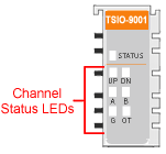
|
State
|
LED
|
Indicates
|
| UP |
Green |
Up Counting Status |
| DN (Down) |
Green |
Down Counting Status |
| A |
Green |
A Phase Input Status |
| B |
Green |
B Phase Input Status |
| G |
Green |
G Phase Input Status |
| OT (Out) |
Green |
Status Output |
|

