|
|
| . |
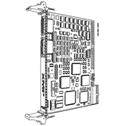
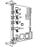
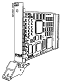
XMP-Analog Controllers:
|
|||||||||||||||||||||||||||||||||||||||||||||||||||||||||||||||||||||||||||||||||||||||||||||||||||||||||||||||||||||||||||||||||||||||||||||||||||
|
Controller |
Voltage 1 |
Current 2
|
Current |
|---|---|---|---|
|
XMP-PCI (analog) 
|
+5 VDC ± 5% |
1.70 (main) |
3.20 (main) |
|
+12 VDC ± 10% |
0.03 (main) |
0.05 (main) |
|
|
-12 VDC ± 10% |
0.01 (main) |
0.01 (main) |
|
|
SIM4 Module on XMP-PCI 
|
+5 VDC ± 5% |
0.18 |
0.40 |
|
+12 VDC ± 10% |
0.01 |
0.01 |
|
|
-12 VDC ± 10% |
0.03 |
0.05 |
|
|
XMP-CPCI-6U (analog) 
|
+3.3 VDC ± 10% |
0.90 (main) |
1.40 (main) |
|
+5 VDC ± 5% |
0.90 (main) |
1.90 (main) |
|
|
+12 VDC ± 10% |
0.03 (main) |
0.05 (main) |
|
|
-12 VDC ± 10% |
0.01 (main) |
0.01 (main) |
|
|
SIM4 Module on XMP-CPCI 
|
+3.3 VDC ± 10% |
0.08 |
0.20 |
|
+5 VDC ± 5% |
0.12 |
0.20 |
|
|
+12 VDC ± 10% |
0.01 |
0.01 |
|
|
-12 VDC ± 10% |
0.03 |
0.05 |
|
|
XMP-SERCOS-CPCI-6U 
|
+3.3 VDC ± 10% |
0.50 |
0.75 |
|
+5 VDC ± 5% |
0.50 |
0.75 |
|
|
XMP-CPCI-3U (analog) 
|
+3.3 VDC ± 10% |
0.50 |
0.90 |
|
+5 VDC ± 5% |
0.45 |
1.15 |
|
|
XMP-SERCOS-PMC 
|
+3.3 VDC ± 10% |
0.375 |
0.50 |
|
+5 VDC ± 5% |
0.375 |
0.50 |
|
|
XMP-SERCOS-PCI-S2 
|
+5 VDC ± 5% |
0.60 |
1.00 |
1. Controller voltage required at computer or card cage.
2. Installed SIM4 modules and encoders also contribute to current demands.
Then make sure that voltage drops in your cabling are NOT a problem. If voltage drops are a problem, power the encoders using an external supply. For every 100 mA of current drawn, the 5V_OUT voltage may drop 0.2 volts or more (due to cable resistance). For example, if two encoders each draw 150 mA, then 5V_OUT may drop to 4.4 volt at the encoders. This could cause your encoder to fail!
SERCOS is a standardized industrial format utilizing fiber-optic technology. The optical power demands of drives vary widely, depending upon the drive itself, length of cables, etc. For more information regarding SERCOS motion drive power demands, please see your drive's manufacturer.
XMP-analog systems rely upon traditional copper wiring to pass analog signals between the drive and controller. Two voltages are available for opto-inputs on XMP controllers: 5VDC and 24VDC. To determine whether your controller supports 5V or 24V, look for a sticker on the XMP circuit board. The sticker will say either "5V" or "24V."
For more detailed information regarding configuration of analog I/O click here. Specifications for transceiver components used in the XMP-Analog controller's I/O are provided in tables below.
|
Description |
Specification |
|
Input High Threshold |
VDIFF > 0.2V |
|
Input Low Threshold |
VDIFF < -0.2V |
|
Input Current |
IIN <
1.0mA @ VIN = 12V NOTE: In addition,
encoder inputs have 100 |
|
Propagation Delay |
Tp < 200 ns |
|
Absolute Maximums 1 |
ESD Protection ± 15kV |
|
Description |
Specification |
|
Differential Output |
VDIFF
< 5V @ I = 0mA |
|
Common Mode |
VOUT
(common mode) < 3V (100 |
|
Propagation Delay |
Tp < 60ns |
|
Absolute Maximums 2 |
IOUT < 50mA |
|
Description |
Specification |
|
Active Input Guaranteed |
IIN
> 2mA |
|
Inactive Input Guaranteed |
VIN < 0.1mA |
|
Propagation Delay |
Tp < 20µs |
|
Absolute Maximums 3 |
5V input (820 |
|
Description |
Specification |
|
Active Output Guaranteed |
VOUT
< 0.3V @ IOUT < 2mA |
|
Inactive Output Guaranteed |
IOUT < 0.01mA |
|
Propagation Delay |
Tp <
100µs (load < 10 k |
|
Absolute Maximums 4 |
IOUT
< 50mA |
|
Description |
Specification |
Active Input Guaranteed |
IIN > 2mA |
|
Input Voltage Threshold |
VIN < 1.7V @ IIN = 2mA |
|
Inactive Input Guaranteed |
IIN < 0.1mA |
|
Propagation Delay |
Tp < 20µs |
|
Absolute Maximums 5 |
IIN
< 50mA |
|
Description |
Specification |
|
Active Output Guaranteed |
VOUT
< 0.3V @ IOUT < 2mA |
|
Inactive Output Guaranteed |
IOUT < 0.01mA |
|
Propagation Delay |
Tp <
100µs (load < 10 k |
|
Absolute Maximums 6 |
IOUT
< 50mA |
| | | Copyright © 2001-2009 Motion Engineering |