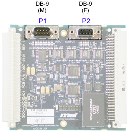
SQIO-ADC4DAC4: Inputs
Characteristics | Application | Pinouts
Characteristics
| |
- The analog inputs are arranged in a bank of 4 with a common analog ground connection.
- The 4 channels are converted sequentially in the order 3 > 2 > 1 > 0. If there is a node or a network that has multiple SQIO-ADC4DAC4 modules then the sequential conversion process will take place simultaneously on all board modules.
|
Parameter |
Value |
Notes |
| Resolution |
16 bits |
— |
Input range
(for an input gain of unity) |
±10V (305µV/bit) |
Min |
| Common mode voltage range |
±5V |
Max |
| Conversion Time |
126µs |
Max |
Common mode rejection ratio
(for an input gain of unity) |
85dB @ 100Hz
60dB @ 4 kHz |
Typical |
| Input filter pole |
34 kHz |
Typical |
| Input Impedence |
10MΩ |
Typical |
| No missing codes |
15 bits |
Typical |
| Integral linearity error |
±3 bits |
Typical |
| Drift of bipolar zero |
±0.13 bits/K |
Typical |
Application
The analog inputs are arranged in a bank of 4.
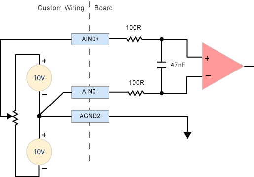
Connecting an ADC channel
Pinouts
For pinout information, see the following pages.
Inputs: P1
Outputs: P2
|

